
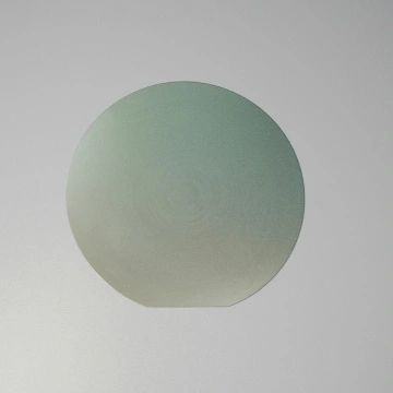
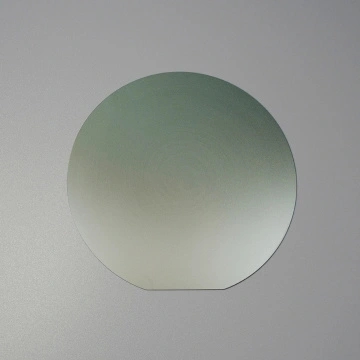
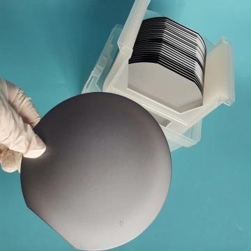
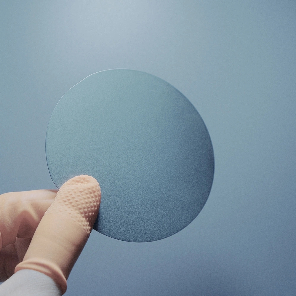
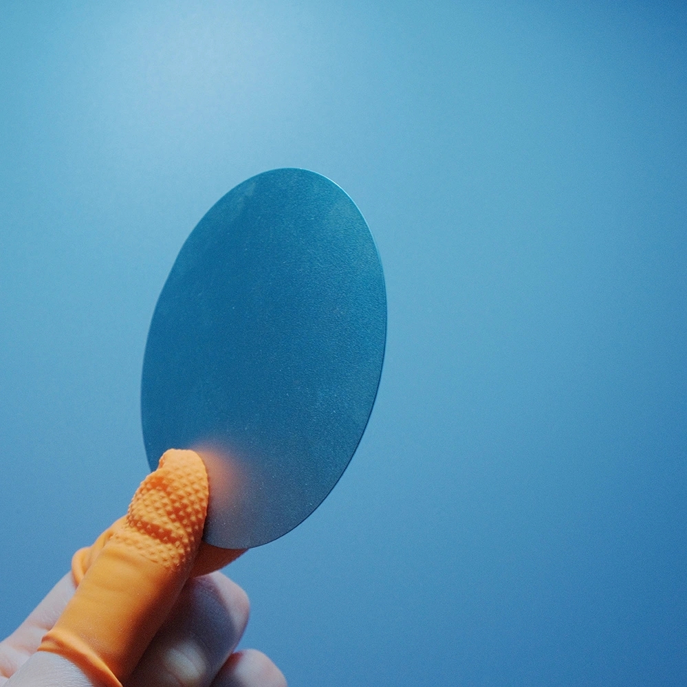
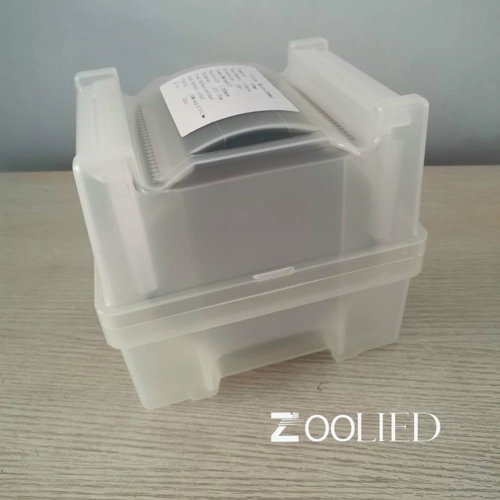
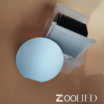
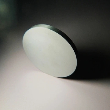
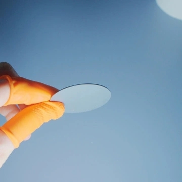
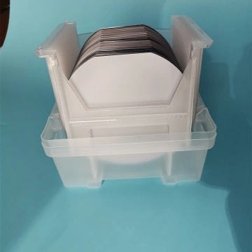
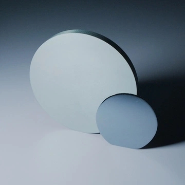
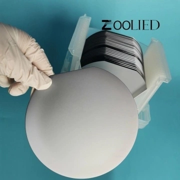
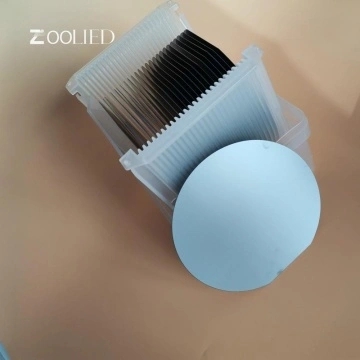
Zoolied 4 Inch Si Wafers (100 mm) , orientation: <100>, resistance: 0.0001-10000 ohm, type: P, circle thickness: 480 microns. Zoolied Silicon Wafers are highly polished, and the smoothness is comparable to that of glass coverslips. As an excellent substrate for SEM and SPM applications, silicon chip substrates are opaque and have low resistivity, which essentially makes them "conductive" in SEM, which involves microamperes in terms of current. They are chemically inert and can be further cleaned before use without worrying about chemical etching effects. They can also be heated at temperatures much higher than glass without change, which makes certain heating experiments possible.
Zoolied offers a variety of optical Glass Wafers, such as Dummy Silicon Wafers, Jgs1 Wafers, and K9 Wafers, and Bk7 Wafers. ZOOLIED provides multiple anti-reflection coating options and also provides uncoated optical glass wafers. Looking for ideal optical si wafers and Ge Wafers Manufacturer & supplier? We have a wide selection at great prices to help you get creative. All the optical glass wafers are quality guaranteed. Zoolied is China Origin Factory of optical Wafers. If you have any question, please feel free to contact us.
Note: Please pay attention to your email at any time after inquiring, we will send you the quotation by email.
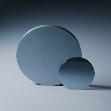
| Zoolied Standard Silicon Wafer | |||||||
| Diameter | 2" | 3" | 4" | 5" | 6" | 8" | 12" |
| Grade | Prime/ Test/ Dummy | ||||||
| Growth Method | CZ/FZ | ||||||
| Orientation | < 100 > , < 111 > , < 110 > | ||||||
| Type/Dopant | P/Boron , N /Phos, N /As, N /Sb | ||||||
| Thickness (um) | 279 | 380 | 525 | 625 | 675 | 725 | 775 |
| Thickness Tolerance | Standard ± 25μm | ||||||
| Resistivity | 0.001 - 10,000ohm-cm | ||||||
| Surface Finished | DSP,SSP | ||||||
| TTV (um) | Standard < 10 um | ||||||
| Bow/Warp (um) | Standard <40 um | ||||||
| Particle | Specified by customer | ||||||


The production of silicon wafer usually has the following steps:
1) long crystal, which can be divided into CZ and FZ, because the fused polycrystalline material will directly contact with the quartz crucible, so the impurities in the quartz crucible will contaminate the fused polycrystalline. The CZ method is suitable for drawing large-diameter (300 mm) silicon wafers, which is the main Semiconductor Silicon Wafer material at present. As the polycrystalline raw materials are not in contact with the quartz crucible, there are few internal defects and low carbon and oxygen content, but the price is expensive and the cost is high. It is suitable for high-power devices and some high-end products.
2) slicing and drawing of the single crystal silicon rod need to cut off the head and tail material, then roll and grind it to the required diameter, cut the flat edge or V groove, and then cut into thin silicon wafer. At present, diamond wire cutting technology is usually used, with high efficiency and good warpage and curvature of silicon wafer. A small number of special shaped pieces can be cut with an inner circle.
3) grinding: after slicing, the damaged layer on the cutting surface needs to be removed by grinding to ensure the quality of the silicon wafer surface, about 50um.
4) corrosion: corrosion is to further remove the damaged layer caused by cutting and grinding, so as to prepare for the following polishing process. Corrosion usually includes alkali corrosion and acid corrosion. At present, due to environmental factors, most of them adopt alkali corrosion. The removal amount of corrosion can reach 30-40um, and the surface roughness can also reach micron level.
5) polishing: polishing is an important process for silicon wafer production. Polishing is to further improve the surface quality of silicon wafer through CMP (chemical mechanical polished) technology, so that it can meet the requirements of chip production. After polishing, the surface roughness is usually RA < 5A.
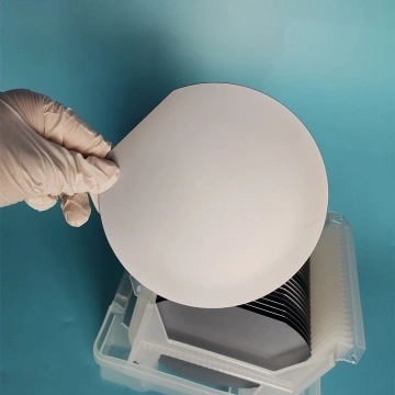
6) cleaning and packaging: as the linewidth of the integrated circuit is getting smaller and smaller, the requirements for improving the particle size index are getting higher and higher. Cleaning and packaging is also an important process for silicon wafer production. Most particles attached to the surface of silicon wafer > 0.3um can be cleaned by megasonic cleaning, and then the silicon wafer surface can be made by vacuum sealing packaging or inert gas packaging with a plug box free of cleaning The surface cleanliness meets the requirements of IC.
-
 DSP 100mm 300um >10000Ω.cm N Silicon wafer
-
 100mm 525um 1-10Ω.cm P Orientation Silicon wafer
-
 100mm 475-575um 3-15Ω.cm P Silicon wafer
-
 DSP 100mm 1000um >10000Ω.cm N Silicon wafer
-
 DSP 50.8mm 400um 3000-5000ohm.cm N Silicon Wafer
-
 DSP 100mm/500um <0.009Ω.cm Silicon wafer
-
 100mm 500um 5000-8000Ω.cm N Silicon wafer
-
 SSP 100mm 500um 1-5Ω.cm N Silicon wafer
