
Wafer Processing | How are Silicon Wafers manufactured? Before semiconductors can be manufactured, silicon must be turned intosilicon wafers. This starts with the growth of silicon ingots. It can take a week to a month to grow a silicon ingot, depending on many factors, including size, quality, and specifications. Let us have a deeper understanding of silicon wafer processing and how they are made.
Ingot growth
To grow a silicon ingot, the first step is to heat the silicon to 1420°C, which is higher than the melting point of silicon. Once the polycrystalline and dopant combination is liquefied, a single silicon crystal, the seed, sits on top of the melt and barely touches the surface. The seed crystal has the same crystal orientation as required for the finished ingot.
slice
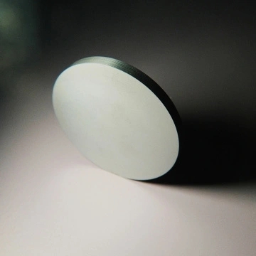
Once the ingot is fully grown, it is ground to a rough diameter slightly larger than the target diameter of the final silicon wafer. After several inspections, the ingot enters the slice. Due to the hardness of silicon, the diamond edge saw carefully cuts the silicon wafers to make them slightly thicker than the target specification.
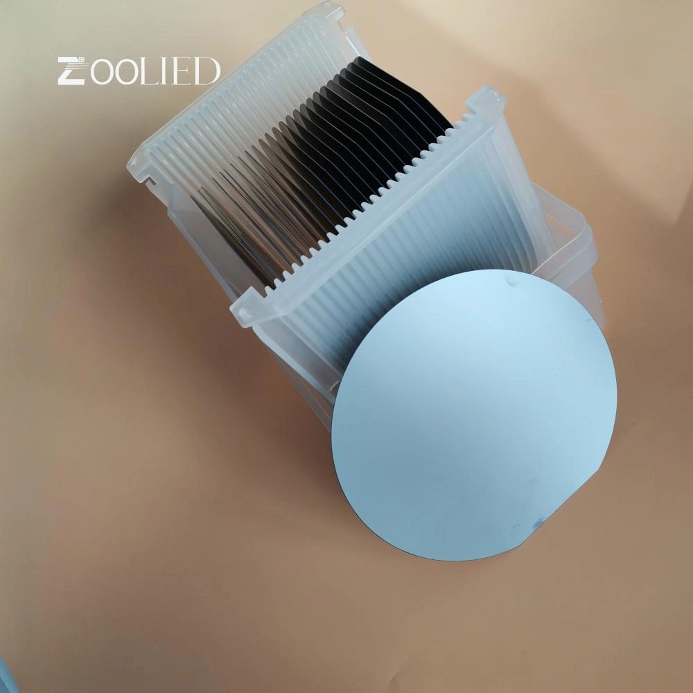
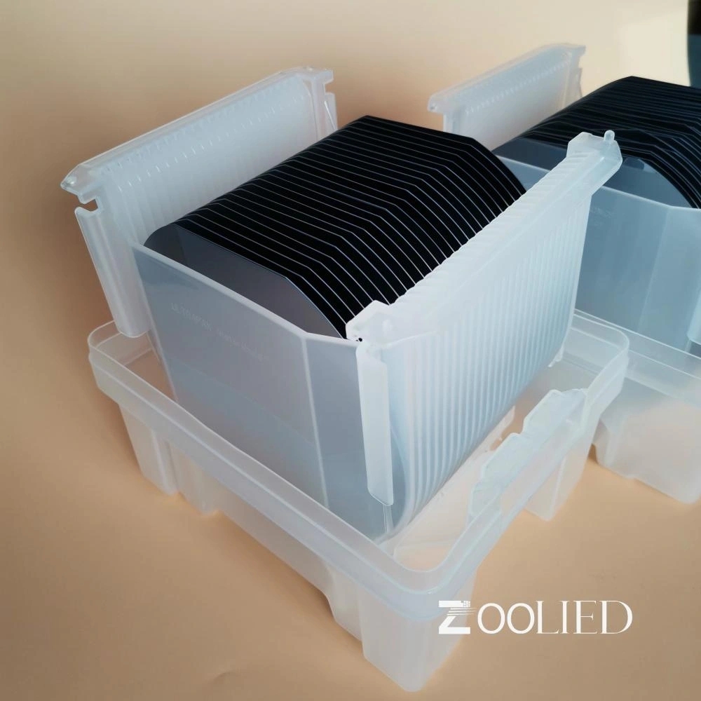
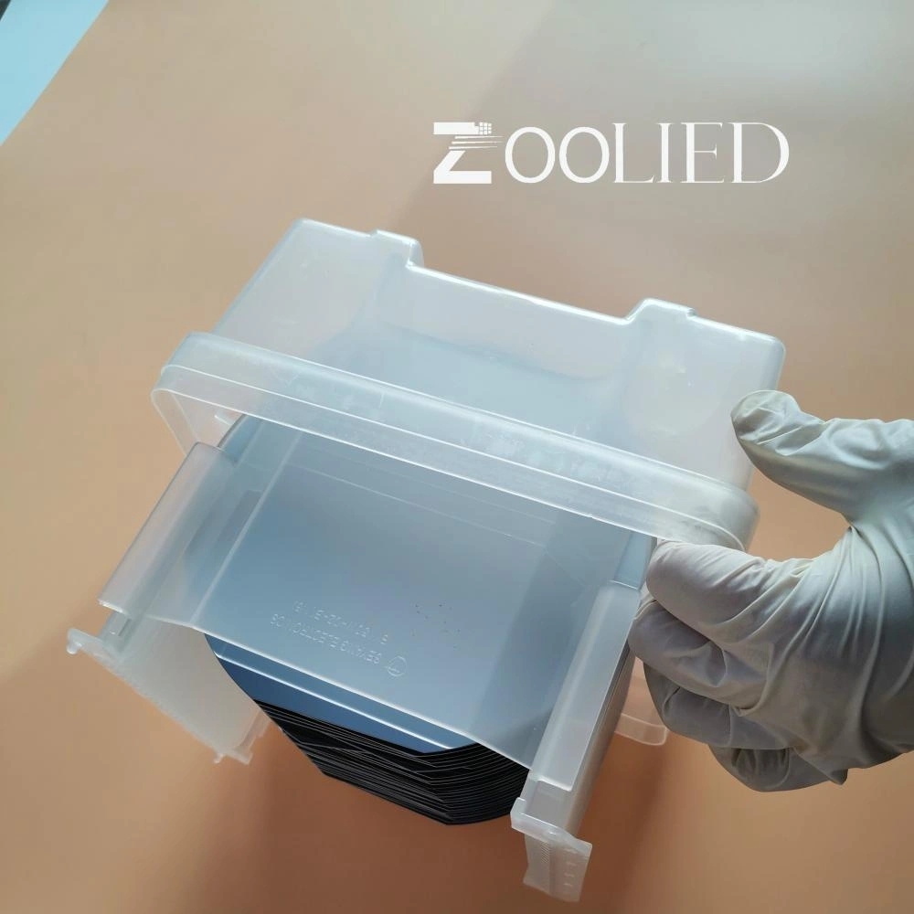
clean
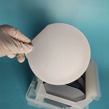
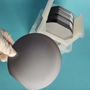
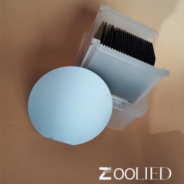
The final and most critical step in the manufacturing process is polishing the wafer. The process is carried out in a clean room. To help maintain this level of cleanliness, workers must wear clean clothes that cover the entire body from head to toe, and do not collect or carry any particles. They are also standing under a fan, which will blow away any small particles that may have accumulated before entering the room.
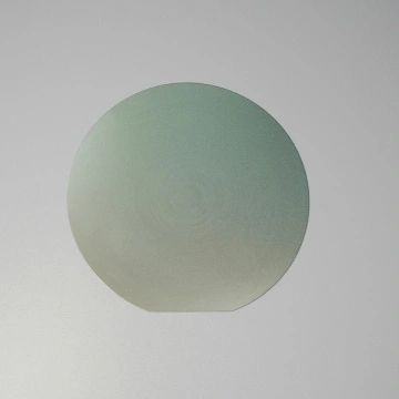
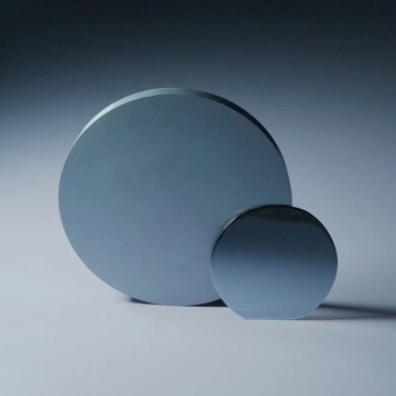
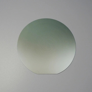
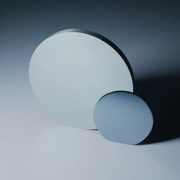
Zoolied offers a variety of optical Glass Wafers, such as Dummy Silicon Wafers, Jgs1 Wafers, and K9 Wafers, and Bk7 Wafers. ZOOLIED provides multiple anti-reflection coating options and also provides uncoated optical glass wafers. Looking for ideal optical si wafers and Ge Wafers Manufacturer & supplier? We have a wide selection at great prices to help you get creative. All the optical glass wafers are quality guaranteed. Zoolied is China Origin Factory of optical Wafers. If you have any question, please feel free to contact us.
Note: Please pay attention to your email at any time after inquiring, we will send you the quotation by email.
| Zoolied Standard Silicon Wafer | |||||||
| Diameter | 2" | 3" | 4" | 5" | 6" | 8" | 12" |
| Grade | Prime/ Test/ Dummy | ||||||
| Growth Method | CZ/FZ | ||||||
| Orientation | < 100 > , < 111 > , < 110 > | ||||||
| Type/Dopant | P/Boron , N /Phos, N /As, N /Sb | ||||||
| Thickness (um) | 279 | 380 | 525 | 625 | 675 | 725 | 775 |
| Thickness Tolerance | Standard ± 25μm | ||||||
| Resistivity | 0.001 - 10,000ohm-cm | ||||||
| Surface Finished | DSP,SSP | ||||||
| TTV (um) | Standard < 10 um | ||||||
| Bow/Warp (um) | Standard <40 um | ||||||
| Particle | Specified by customer | ||||||


-
 SSP 100mm 1000um >10000Ω.cm N Silicon wafer
-
 100mm 500um Silicon wafer
-
 SSP 100mm 525um 0.002-0.003Ω.cm N Silicon wafer
-
 DSP 4" 1000um >10000Ω.cm N Semiconductor Silicon w...
-
 DSP 50.8mm 500um >10000ohm.cm Intrinsic Silicon Wa...
-
 DSP 100mm 300um >10000Ω.cm N Silicon wafer
-
 100mm 525um 1-10Ω.cm P Orientation Silicon wafer
-
 100mm 475-575um 3-15Ω.cm P Silicon wafer
