Si Windows and Lenses
-
 D10mm T1mm - 2mm Silicon (Si) Windows Typical Applications
Thermal imaging
Si Crytal Lens and windows are often used for NIR and MWIR thermal imaging applications. Though the image quality may not be as sup... Contact Now Click for details -
 D30mm T2mm Infrared Silicon with BBAR@3-5μm Windows Lwir Ge Windows are ideal for IR applications at a long range of wavelengths, including use in lower power CO2 lasers. Germanium also has low dispersion, ideal for imaging ... Contact Now Click for details
-
 IR Silicon with BBAR & DLC@3-5μm Si Windows Zoolied’s Lwir Ge Windows with Diamond-Like Carbon (DLC) coating have been designed with durability in mind. Featuring a high efficiency broadband anti-reflection coating o... Contact Now Click for details
-
 D25mm Infrared Silicon with BBAR@3-5μm Windows Lwir Ge Windows and IR Ge windows are commonly used in defence and aerospace industries, life and medical sciences, industrial OEM and many other infrared applications.
Z... Contact Now Click for details -
 Silicon Germanium Window with DLC for outdoor cameras Si Crytal Lens and window are ideal choice for applications using wavelengths in the near-IR range and parts of the mid-IR range.The big Silicon Windows offers high thermal... Contact Now Click for details
-
 Silicon lens and windows 4-12μm T>80% for LWIR Zoolied's big Silicon Windows manufactured from optical grade silicon are popular for the 1.2 - 7μm spectral region due to their low cost and low density. Due to Si Crytal ... Contact Now Click for details
-
 Silicon Ge for 8-14μm infrared temperature measurement Every Single Crystal Ir Germanium has high index of refraction (around 4.0 from 2 - 14μm), an anti-reflection coating, such as Germanium with DLC COATING or BBAR COATING, i... Contact Now Click for details
-
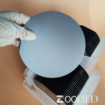 50.8mm SSP 430um >10000Ω.cm N<100> Silicon wafer Semiconductors are the core of electronic products, the cornerstone of the information industry, and are also known as the "food" of modern industry. But how much do we kno... Contact Now Click for details
-
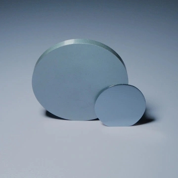 50.8mm SSP 430um 8000-10000Ω.cm N<100> Silicon wafer Commonly used sizes of Silicon Wafers include 4, 6, 8, 12 inches. At present, in the application of semiconductors, the mainstream is mainly 8-inch and 12-inch large silico... Contact Now Click for details
-
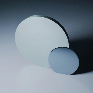 50.8m SSP 430um 3000-5000Ω.cm N<100> Silicon wafer Commonly used sizes of Silicon Wafers include 4, 6, 8, 12 inches. At present, in the application of semiconductors, the mainstream is mainly 8-inch and 12-inch large silico... Contact Now Click for details
-
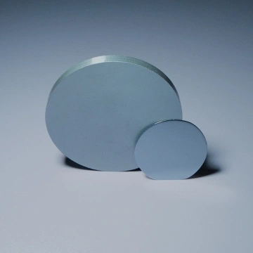 SSP 50.8mm 430um 1000-3000 ohm.cm N <100> Silicon Wafer The silicon content of 25.8% in the earth's crust provides an inexhaustible source for the production of monocrystalline silicon. Since silicon is one of the most abundant ... Contact Now Click for details
-
 SSP 50.8mm 450um >1ohm.cm P<111> Silicon wafer The silicon content of 25.8% in the earth's crust provides an inexhaustible source for the production of monocrystalline silicon. Since silicon is one of the most abundant ... Contact Now Click for details
-
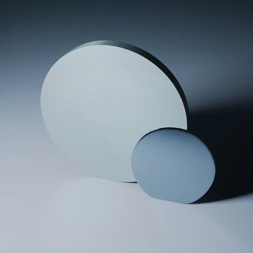 N Type Orientation <111> Silicon Wafer Zoolied Semiconductor DSP 50.8mm Thin Si Wafers are manufactured by cutting, polishing and cleaning single crystals of high-purity silicon under a strict production and qua... Contact Now Click for details
-
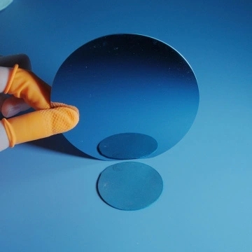 2 Semiconductors are the core of electronic products, the cornerstone of the information industry, and are also known as the "food" of modern industry. But how much do we kno... Contact Now Click for details
-
 3 inch T500um Silicon Wafer Semiconductors are the core of electronic products, the cornerstone of the information industry, and are also known as the "food" of modern industry. But how much do we kno... Contact Now Click for details