
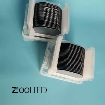
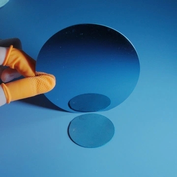
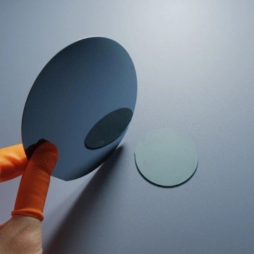
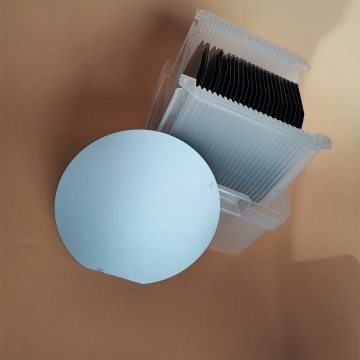
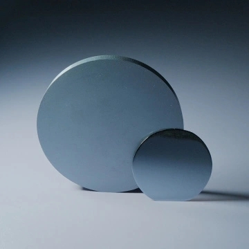


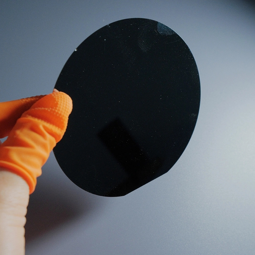
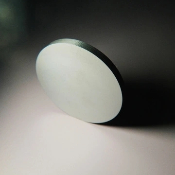
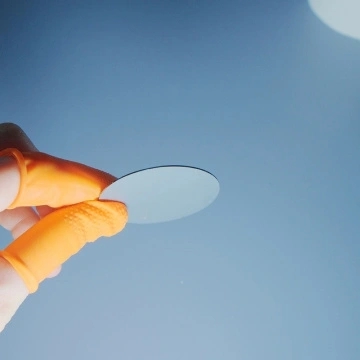
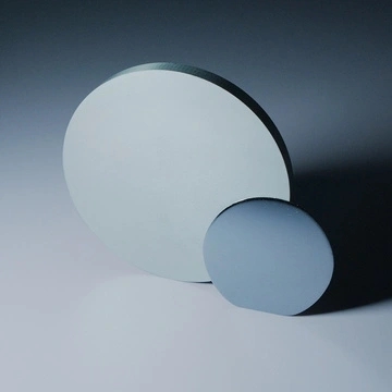
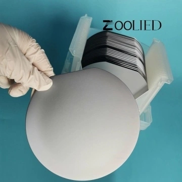
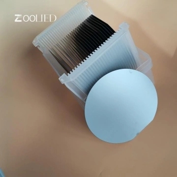
Silicon Wafers & Semiconductor Wafers: a wafer is a fairly thin disc of a semiconductor material such as silicon. It is used as a support for the manufacture of microstructures by techniques such as etching, doping, deposition of other materials (epitaxy, sputtering, chemical vapor deposition, etc.) and photolithography. These micro-structures are a major component in the manufacture of integrated circuits, transistors, power semiconductors. The wafers can be of different sizes from 1 inch (25.4 mm) up to 300 mm for a thickness of the order of 0.7 mm. The trend is to use the largest wafers possible to be able to burn more chips simultaneously and limit losses on the edge of the plate, resulting in increased production at a lower cost. This orientation is important because the crystals have anisotropic structural and electronic properties. We print integrated circuits, transistors, and power semiconductors on these tight grid Thin Si Wafers to put as much as possible on a single silicon or semiconductor wafer.
Zoolied offers a variety of optical Glass Wafers, such as Dummy Silicon Wafers, Jgs1 Wafers, and K9 Wafers, and Bk7 Wafers. ZOOLIED provides multiple anti-reflection coating options and also provides uncoated optical glass wafers. Looking for ideal optical si wafers and Ge Wafers Manufacturer & supplier? We have a wide selection at great prices to help you get creative. All the optical glass wafers are quality guaranteed. Zoolied is China Origin Factory of optical Wafers. If you have any question, please feel free to contact us.
Note: Please pay attention to your email at any time after inquiring, we will send you the quotation by email.
| Zoolied Standard Silicon Wafer | |||||||
| Diameter | 2" | 3" | 4" | 5" | 6" | 8" | 12" |
| Grade | Prime/ Test/ Dummy | ||||||
| Growth Method | CZ/FZ | ||||||
| Orientation | < 100 > , < 111 > , < 110 > | ||||||
| Type/Dopant | P/Boron , N /Phos, N /As, N /Sb | ||||||
| Thickness (um) | 279 | 380 | 525 | 625 | 675 | 725 | 775 |
| Thickness Tolerance | Standard ± 25μm | ||||||
| Resistivity | 0.001 - 10,000ohm-cm | ||||||
| Surface Finished | DSP,SSP | ||||||
| TTV (um) | Standard < 10 um | ||||||
| Bow/Warp (um) | Standard <40 um | ||||||
| Particle | Specified by customer | ||||||


-
 DSP 100mm 300um >10000Ω.cm N Silicon wafer
-
 100mm 525um 1-10Ω.cm P Orientation Silicon wafer
-
 100mm 475-575um 3-15Ω.cm P Silicon wafer
-
 DSP 100mm 1000um >10000Ω.cm N Silicon wafer
-
 DSP 50.8mm 400um 3000-5000ohm.cm N Silicon Wafer
-
 DSP 100mm/500um <0.009Ω.cm Silicon wafer
-
 100mm 500um 5000-8000Ω.cm N Silicon wafer
-
 SSP 100mm 500um 1-5Ω.cm N Silicon wafer
