
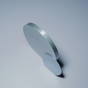
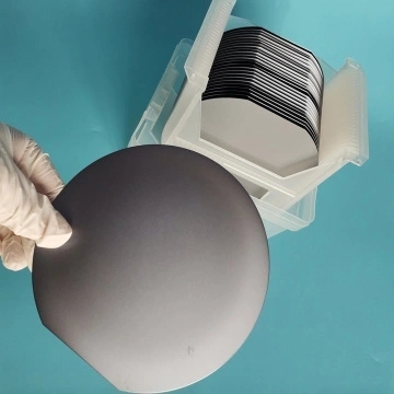
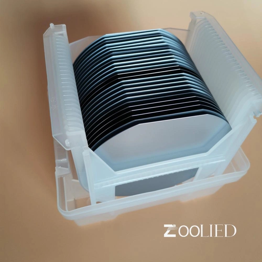
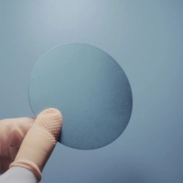
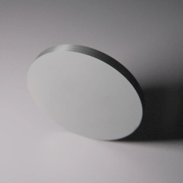
Silicon is the second most common element in the earth’s crust, comprising about 26% and exceeded only by oxygen at 49%. However, silicon does not naturally exist in the pure form required for electronic applications. The starting material is silica sand with a concentration of quartz (silicon dioxide) as high as 95%. The application of Silicon Wafers covers almost every aspect of our lives and is the basis of electronic "chips". The wide range of new applications in the Internet of Things, wearable and mobile devices, autonomous vehicles, cloud computing, 5G communication networks and other fields actually ensures that the demand for Thin Si Wafers will continue to accelerate growth.
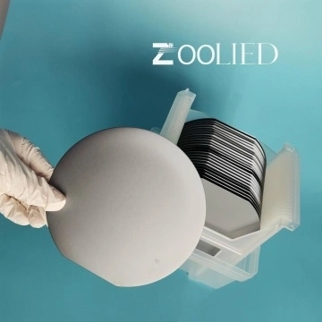
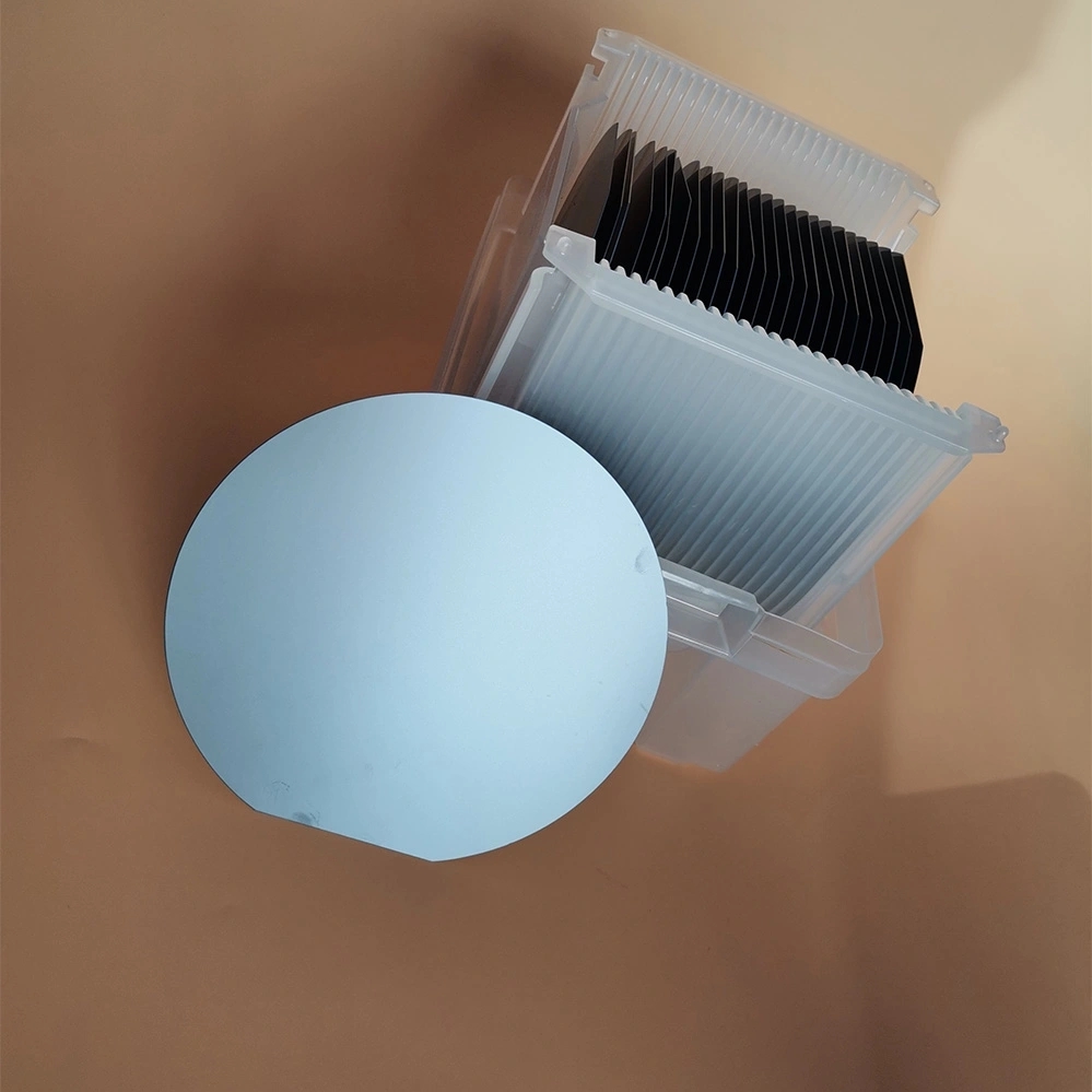
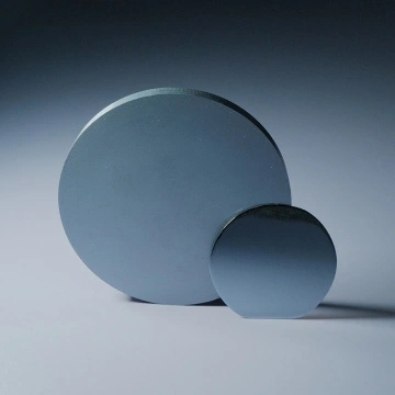
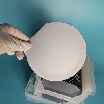
Zoolied offers a variety of optical Glass Wafers, such as Dummy Silicon Wafers, Jgs1 Wafers, and K9 Wafers, and BK8 wafers. Zoolied provides multiple anti-reflection coating options and also provides uncoated optical glass wafers. Looking for ideal optical si wafers and Ge Wafers Manufacturer & supplier? We have a wide selection at great prices to help you get creative. All the optical glass wafers are quality guaranteed. Zoolied is China Origin Factory of optical Wafers. If you have any question, please feel free to contact us.
Note: Please pay attention to your email at any time after inquiring, we will send you the quotation by email.
| Zoolied Standard Silicon Wafer | |||||||
| Diameter | 2" | 3" | 4" | 5" | 6" | 8" | 12" |
| Grade | Prime/ Test/ Dummy | ||||||
| Growth Method | CZ/FZ | ||||||
| Orientation | < 100 > , < 111 > , < 110 > | ||||||
| Type/Dopant | P/Boron , N /Phos, N /As, N /Sb | ||||||
| Thickness (um) | 279 | 380 | 525 | 625 | 675 | 725 | 775 |
| Thickness Tolerance | Standard ± 25μm | ||||||
| Resistivity | 0.001 - 10,000ohm-cm | ||||||
| Surface Finished | DSP,SSP | ||||||
| TTV (um) | Standard < 10 um | ||||||
| Bow/Warp (um) | Standard <40 um | ||||||
| Particle | Specified by customer | ||||||


-
 200mm T0.1mm 100um Polished Silicon wafer
-
 High quality DSP N Silicon wafer
-
 100mm 1000um 1-10Ω.cm N Silicon wafer
-
 SSP 100mm/1000um >10000Ω.cm N Silicon wafer
-
 SSP 50.8mm 450um>1Ω.cm PSilicon wafer
-
 50.8mm 525um 0-100Ω.cm P Silicon wafer
-
 SSP 1-5Ω.cm N Orientation Silicon wafer
-
 76.2mm 380um >20000Ω.cm N Silicon wafer
