
.jpg)
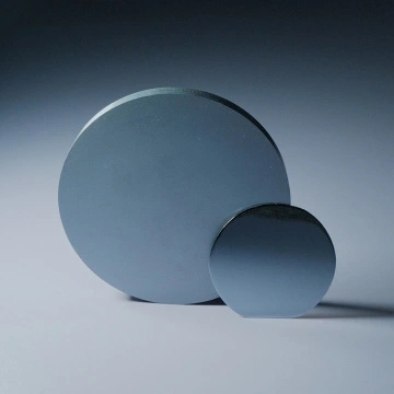
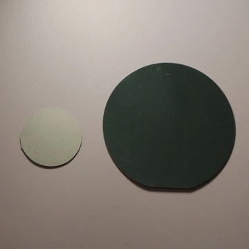
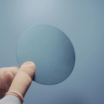
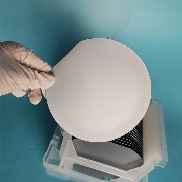
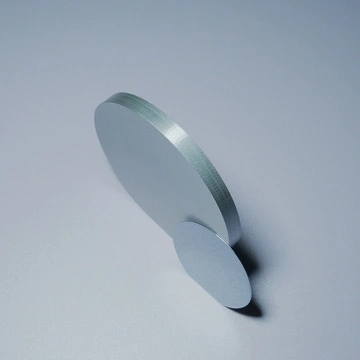
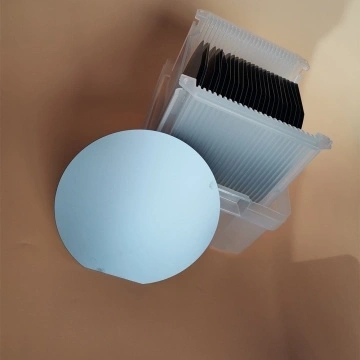
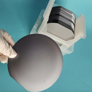
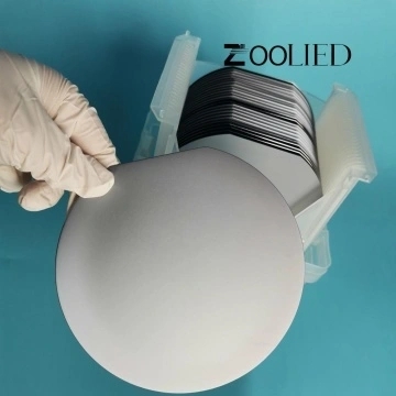
The production of Silicon Wafers usually has the following steps: the silicon wafers manufacturing process includes crystal pulling, scribing, grinding, chamfering, etching, polishing, cleaning and inspection, among which crystal pulling, polishing wafer and inspection are the core links of silicon wafer manufacturing. As a basic semiconductor substrate, silicon wafers must have high standards of purity, surface flatness, cleanliness, and impurity contamination in order to maintain the original design functions of the chip. The high specification requirements of semiconductor silicon wafers complicate the manufacturing process. The four core steps include polysilicon purification and polysilicon ingot casting, monocrystalline Thin Si Wafers growth, silicon wafer cutting and shaping. As the raw material of the fab, the quality of the silicon wafer directly determines the stability of the wafer application process. Large-size silicon wafers have become the development trend of silicon wafers in the future. In order to improve production efficiency and reduce costs, more and more large-size silicon wafers are used.
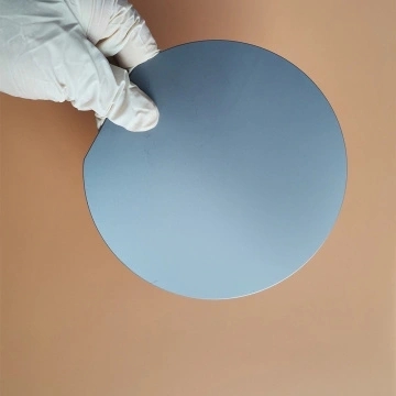
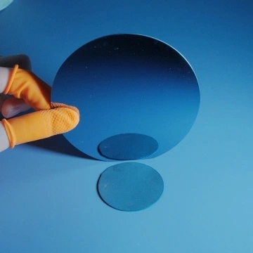
Zoolied offers a variety of optical Glass Wafers, such as Dummy Silicon Wafers, Jgs1 Wafers, and K9 Wafers, and BK8 wafers. ZOOLIED provides multiple anti-reflection coating options and also provides uncoated optical glass wafers. Looking for ideal optical si wafers and Ge Wafers Manufacturer & supplier? We have a wide selection at great prices to help you get creative. All the optical glass wafers are quality guaranteed. Zoolied is China Origin Factory of optical Wafers. If you have any question, please feel free to contact us.
Note: Please pay attention to your email at any time after inquiring, we will send you the quotation by email.
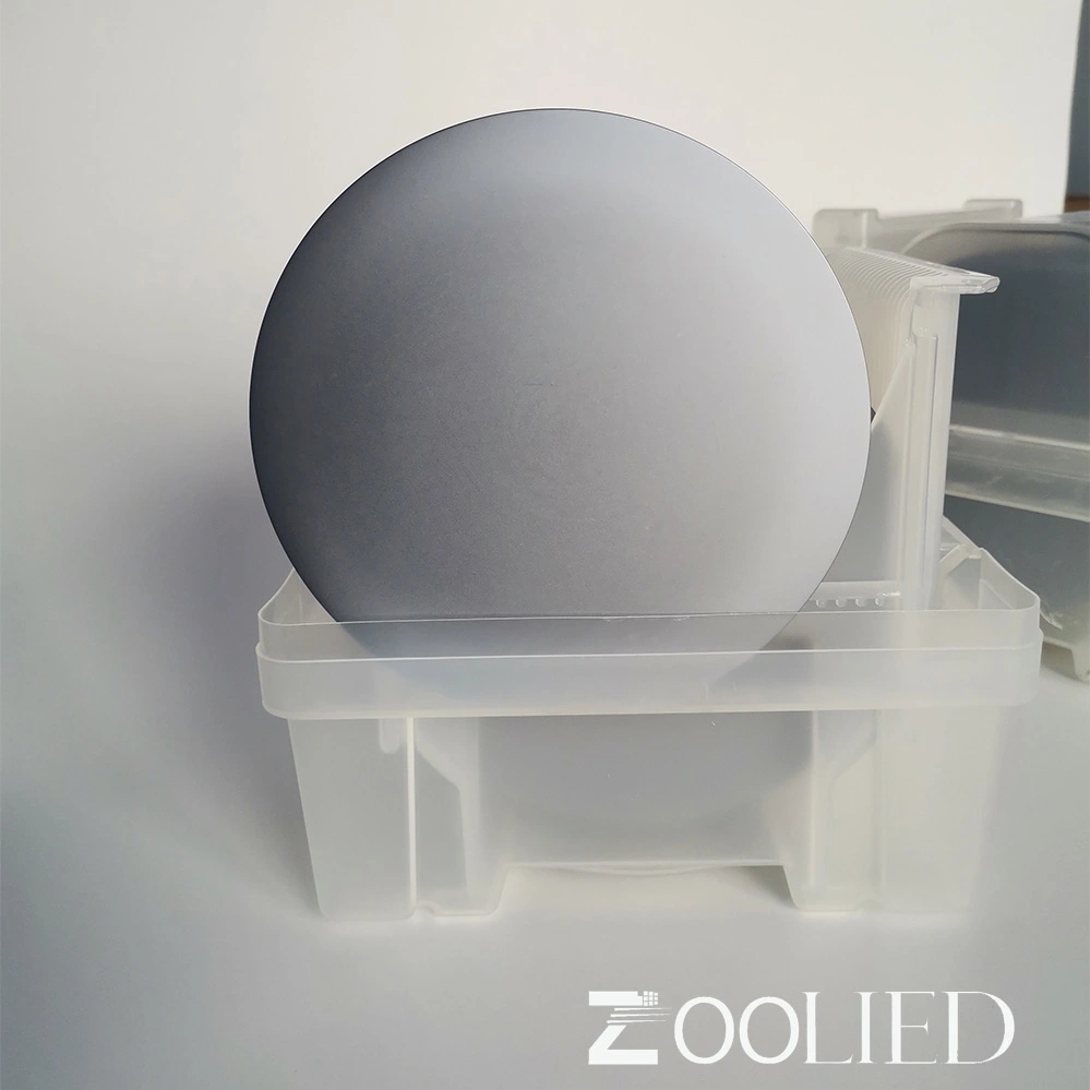
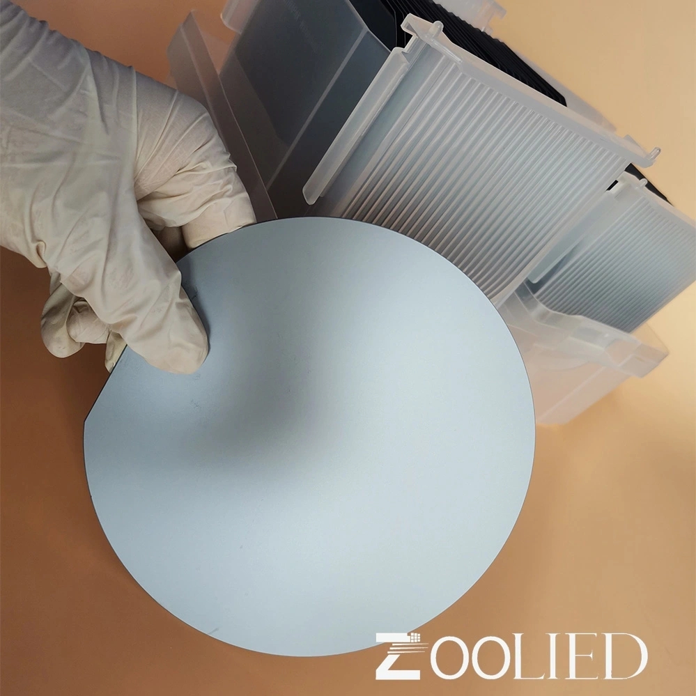
| Zoolied Standard Silicon Wafer | |||||||
| Diameter | 2" | 3" | 4" | 5" | 6" | 8" | 12" |
| Grade | Prime/ Test/ Dummy | ||||||
| Growth Method | CZ/FZ | ||||||
| Orientation | < 100 > , < 111 > , < 110 > | ||||||
| Type/Dopant | P/Boron , N /Phos, N /As, N /Sb | ||||||
| Thickness (um) | 279 | 380 | 525 | 625 | 675 | 725 | 775 |
| Thickness Tolerance | Standard ± 25μm | ||||||
| Resistivity | 0.001 - 10,000ohm-cm | ||||||
| Surface Finished | DSP,SSP | ||||||
| TTV (um) | Standard < 10 um | ||||||
| Bow/Warp (um) | Standard <40 um | ||||||
| Particle | Specified by customer | ||||||


-
 DSP 100mm 360um 2-3Ω.cm N Silicon wafer
-
 SSP 100mm 500um Silicon wafer
-
 100mm 500um Silicon wafer
-
 SSP 100mm 500um 1-10Ω.cm N Silicon wafer
-
 SSP 50.8mm 420um >2000Ω.cm N Silicon wafer
-
 SSP 50.8mm 500um 5000-8000Ω.cm N Silicon wafer
-
 SSP 76.2mm 380um 1-10Ω.cm P Silicon wafer
-
 DSP 150mm 530um >5Ω.cm P Silicon wafer
