
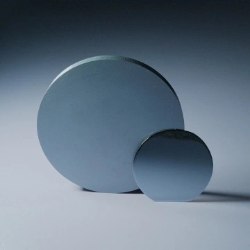

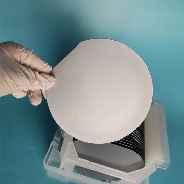
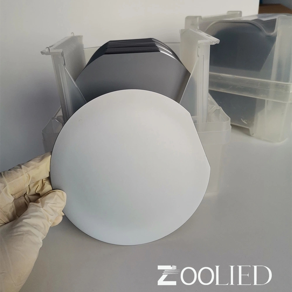

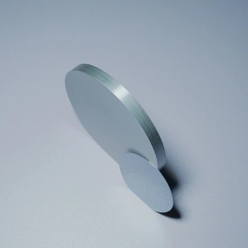
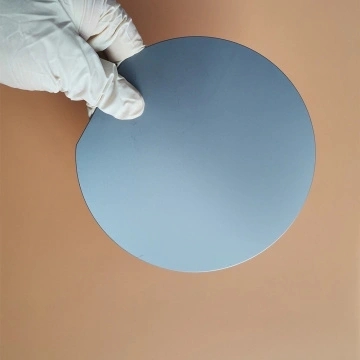
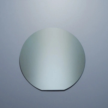
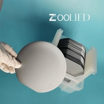
A silicon wafer is a thin slice of pure silicon or doped silicon cut from a silicon ingot. The thickness of the Silicon Wafers range from a few millimeters to a few microns, and can be adjusted according to the application through a thinning process. Zoolied offers a variety of silicon wafers:
Monocrystalline Silicon: (also called single crystal silicon wafer) Is formed of one large single Thin Si Wafers. Silicon ingots are grown with either CZ or FZ technique.
Premium Grade Silicon wafers: (also called Prime Grade Silicon Wafers) are used for production. They are required to be free of dust, particles, chemical heterogeneities, and polishing faults. “Prime” refers to the highest possible grade of a silicon wafer.
Test Grade Silicon Wafers: Used in process monitoring or testing. While Test Grade Silicon wafers have the same chemical characteristics and are enough for testing production, they may contain some defects such as minor polishing faults.
SOI wafers: A Silicon on Insulator wafer is a layered Silicon--Insulator--Silicon substrate. The oxide layer is used as an etch stop or a dielectric layer. ranges from a few millimeters to a few microns, and can be adjusted according to the application through a thinning process. Zoolied offers a variety of silicon wafers:
Monocrystalline Silicon: (also called single crystal silicon wafer) Is formed of one large single thin Si wafers. Silicon ingots are grown with either CZ or FZ technique.
Premium Grade Silicon wafers: (also called Prime Grade Silicon Wafers) are used for production. They are required to be free of dust, particles, chemical heterogeneities, and polishing faults. “Prime” refers to the highest possible grade of a silicon wafer.
Test Grade Silicon Wafers: Used in process monitoring or testing. While Test Grade Silicon wafers have the same chemical characteristics and are enough for testing production, they may contain some defects such as minor polishing faults.
SOI wafers: A Silicon on Insulator wafer is a layered Silicon--Insulator--Silicon substrate. The oxide layer is used as an etch stop or a dielectric layer.
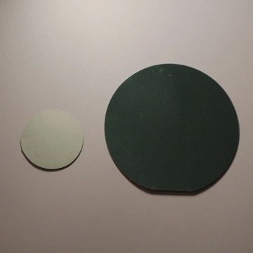
Zoolied offers a variety of optical Glass Wafers, such as Dummy Silicon Wafers, Jgs1 Wafers, and K9 Wafers, and BK8 wafers. Zoolied provides multiple anti-reflection coating options and also provides uncoated optical glass wafers. Looking for ideal optical si wafers and Ge Wafers Manufacturer & supplier? We have a wide selection at great prices to help you get creative. All the optical glass wafers are quality guaranteed. Zoolied is China Origin Factory of optical Wafers. If you have any question, please feel free to contact us.
Note: Please pay attention to your email at any time after inquiring, we will send you the quotation by email.
| Zoolied Standard Silicon Wafer | |||||||
| Diameter | 2" | 3" | 4" | 5" | 6" | 8" | 12" |
| Grade | Prime/ Test/ Dummy | ||||||
| Growth Method | CZ/FZ | ||||||
| Orientation | < 100 > , < 111 > , < 110 > | ||||||
| Type/Dopant | P/Boron , N /Phos, N /As, N /Sb | ||||||
| Thickness (um) | 279 | 380 | 525 | 625 | 675 | 725 | 775 |
| Thickness Tolerance | Standard ± 25μm | ||||||
| Resistivity | 0.001 - 10,000ohm-cm | ||||||
| Surface Finished | DSP,SSP | ||||||
| TTV (um) | Standard < 10 um | ||||||
| Bow/Warp (um) | Standard <40 um | ||||||
| Particle | Specified by customer | ||||||


-
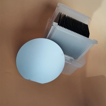
 DSP 100mm 360um 2-3Ω.cm N Silicon wafer
-
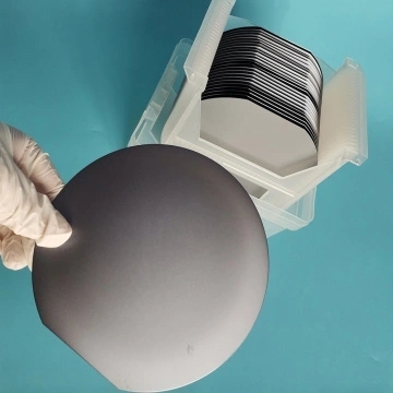
 SSP 100mm 500um Silicon wafer
-
 100mm 500um Silicon wafer
-
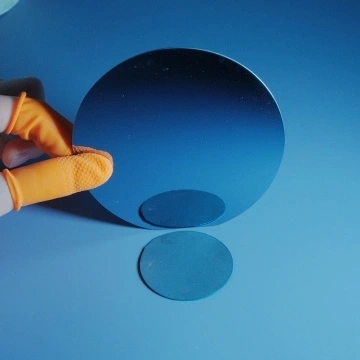
 SSP 100mm 500um 1-10Ω.cm N Silicon wafer
-
 SSP 50.8mm 420um >2000Ω.cm N Silicon wafer
-
 SSP 50.8mm 500um 5000-8000Ω.cm N Silicon wafer
-
 SSP 76.2mm 380um 1-10Ω.cm P Silicon wafer
-
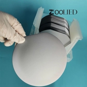 DSP 150mm 530um >5Ω.cm P Silicon wafer
