Lenses and Micro-Nano Optics
2026-4-29
The iteration of optical technology has always been inseparable from breakthroughs in optical components. From traditional spherical lenses to micro-nano optical devices, optical components, as the core carriers of light field manipulation, have driven the upgrading of fields such as optoelectronic imaging, semiconductor detection, and laser applications towards precision, miniaturization, and integration. Among them, components such as lenses, optical windows, filters, and microlens arrays connect the development paths of traditional optics and micro-nano optics, becoming key supports for independent optical substitution.
I. Traditional Lenses
Traditional lenses (spherical and aspherical) rely on the law of refraction of light and utilize the curvature design of optical materials (BK7 glass, quartz, ZnSe, CaF₂, silicon, and other infrared crystals) to achieve beam convergence, collimation, and imaging. They are the core components of various optical systems. As the most widely used optical element, the performance of traditional lenses directly determines the accuracy of the system. Their core advantages lie in mature manufacturing processes, high spectral transmittance, strong environmental adaptability, and suitability for the entire visible, near-infrared, and far-infrared wavelength range.
Combining Zoolied's core products, a complete supply chain has been formed for traditional lenses and supporting optical components: infrared lenses use high-precision crystal substrates such as ZnSe and CaF₂, which are ground and polished with ultra-precision grinding and polishing, and are compatible with laser processing and infrared thermal imaging equipment.
Optical windows, as protective components, combined with custom anti-reflection coatings, achieve high light transmittance and low reflection, and are widely used in semiconductor detection optical paths;
The filter achieves narrowband pass and cutoff filtering through precise spectral selection, working in conjunction with the lens to purify the light field.
However, traditional lenses also have inherent limitations: multiple lenses need to be cemented together to correct chromatic aberration and spherical aberration, resulting in a bulky system; a single lens has a limited function and cannot simultaneously meet the complex requirements of filtering, polarization control, etc., making it difficult to adapt to miniaturized optoelectronic devices.
II. Micro-nano Optics
Micro-nano optics, with its core focus on subwavelength scale structures, breaks free from the physical constraints of traditional lenses. By modifying the surface of optical elements through micro-nano fabrication technology, it achieves more precise and integrated control of the light field. Its core logic is to no longer rely on the refraction due to thickness differences in optical elements, but instead to fabricate nanoarray structures on the surface of substrates such as lenses and windows. By leveraging structural resonance and geometric phase to control the phase, amplitude, and spectrum of light, it enables functional upgrades to traditional optical elements.
Current mainstream micro/nano optical components:
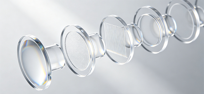
1. Metalens: Nanopillar arrays are fabricated on the surface of substrates such as optical glass and quartz to replace traditional curved lenses. With a thickness of only micrometers, they can integrate achromatic and polarization filtering functions. Combined with filter structures, they can achieve "one-piece integration of multiple functions" and are suitable for AR/VR and miniature imaging devices.
2. Microlens array (MLA): Composed of a large number of micron-sized microlens units, it works in conjunction with traditional lenses and filters to achieve beam homogenization and large field of view imaging. It is widely used in laser beam homogenization and machine vision backlight systems, and is a core integrated component in consumer electronics and semiconductor testing.
3. Micro-nano modified optical components: Micro-nano coated structures are prepared on the surface of traditional infrared windows and lenses to improve light transmittance and reduce reflection loss, while also giving them scratch resistance and corrosion resistance, making them suitable for harsh industrial environments, especially for high-end applications such as infrared sensing and wafer inspection.
III. Integrated Application of Optical Components
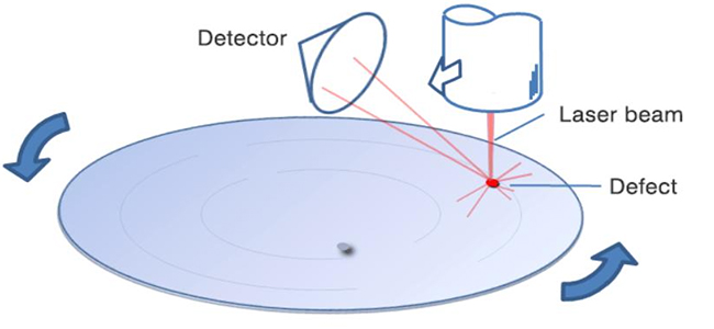
In the field of semiconductor inspection, high-precision aspherical lenses, combined with micro-nano filters and infrared windows, form an inspection optical path to achieve high-resolution identification of wafer defects.
In laser equipment, traditional infrared lenses provide a wide-band, high-transmittance substrate, while micro- and nano-structures enable beam shaping and spectral calibration, improving the precision of laser processing. A complete industrial chain layout of "traditional optical elements + micro- and nano-modification" has been achieved, from the preparation of crystal substrates such as ZnSe and CaF₂, to the precision processing of lenses, windows, and filters, and then to micro- and nano-coating and nano-structure modification, forming a complete industrial chain.
Comparison table of traditional optical elements and micro/nano modified optical elements
In the future, the integration path of using traditional precision optical components as carriers and micro-nano structures as enablers will become the core direction for independent substitution in the high-end optoelectronic field, and promote the application of optical technology in more high-end scenarios.
I. Traditional Lenses
Traditional lenses (spherical and aspherical) rely on the law of refraction of light and utilize the curvature design of optical materials (BK7 glass, quartz, ZnSe, CaF₂, silicon, and other infrared crystals) to achieve beam convergence, collimation, and imaging. They are the core components of various optical systems. As the most widely used optical element, the performance of traditional lenses directly determines the accuracy of the system. Their core advantages lie in mature manufacturing processes, high spectral transmittance, strong environmental adaptability, and suitability for the entire visible, near-infrared, and far-infrared wavelength range.
Combining Zoolied's core products, a complete supply chain has been formed for traditional lenses and supporting optical components: infrared lenses use high-precision crystal substrates such as ZnSe and CaF₂, which are ground and polished with ultra-precision grinding and polishing, and are compatible with laser processing and infrared thermal imaging equipment.
Optical windows, as protective components, combined with custom anti-reflection coatings, achieve high light transmittance and low reflection, and are widely used in semiconductor detection optical paths;
The filter achieves narrowband pass and cutoff filtering through precise spectral selection, working in conjunction with the lens to purify the light field.
However, traditional lenses also have inherent limitations: multiple lenses need to be cemented together to correct chromatic aberration and spherical aberration, resulting in a bulky system; a single lens has a limited function and cannot simultaneously meet the complex requirements of filtering, polarization control, etc., making it difficult to adapt to miniaturized optoelectronic devices.
II. Micro-nano Optics
Micro-nano optics, with its core focus on subwavelength scale structures, breaks free from the physical constraints of traditional lenses. By modifying the surface of optical elements through micro-nano fabrication technology, it achieves more precise and integrated control of the light field. Its core logic is to no longer rely on the refraction due to thickness differences in optical elements, but instead to fabricate nanoarray structures on the surface of substrates such as lenses and windows. By leveraging structural resonance and geometric phase to control the phase, amplitude, and spectrum of light, it enables functional upgrades to traditional optical elements.
Current mainstream micro/nano optical components:
1. Metalens: Nanopillar arrays are fabricated on the surface of substrates such as optical glass and quartz to replace traditional curved lenses. With a thickness of only micrometers, they can integrate achromatic and polarization filtering functions. Combined with filter structures, they can achieve "one-piece integration of multiple functions" and are suitable for AR/VR and miniature imaging devices.
2. Microlens array (MLA): Composed of a large number of micron-sized microlens units, it works in conjunction with traditional lenses and filters to achieve beam homogenization and large field of view imaging. It is widely used in laser beam homogenization and machine vision backlight systems, and is a core integrated component in consumer electronics and semiconductor testing.
3. Micro-nano modified optical components: Micro-nano coated structures are prepared on the surface of traditional infrared windows and lenses to improve light transmittance and reduce reflection loss, while also giving them scratch resistance and corrosion resistance, making them suitable for harsh industrial environments, especially for high-end applications such as infrared sensing and wafer inspection.
III. Integrated Application of Optical Components
In the field of semiconductor inspection, high-precision aspherical lenses, combined with micro-nano filters and infrared windows, form an inspection optical path to achieve high-resolution identification of wafer defects.
In laser equipment, traditional infrared lenses provide a wide-band, high-transmittance substrate, while micro- and nano-structures enable beam shaping and spectral calibration, improving the precision of laser processing. A complete industrial chain layout of "traditional optical elements + micro- and nano-modification" has been achieved, from the preparation of crystal substrates such as ZnSe and CaF₂, to the precision processing of lenses, windows, and filters, and then to micro- and nano-coating and nano-structure modification, forming a complete industrial chain.
Comparison table of traditional optical elements and micro/nano modified optical elements
|
Comparison Dimensions |
Traditional optical elements (lenses/windows/filters) |
Micro/nano modified optical elements |
|
Structural Form |
Most are curved or spherical in shape, are bulky, and require multiple pieces to be assembled |
Planar design, thin (micrometer level), can be integrated into a single chip for multiple functions |
|
Optical Performance |
It has moderate light transmittance and suffers from some reflection loss; multiple elements must be combined to correct aberrations |
High light transmittance (≥90%), low reflection loss, and no need for multi-element correction |
|
Suitable scenarios |
General industrial applications and basic optical inspection, with low requirements for size and integration |
High-end semiconductor testing, AR/VR, precision instruments, and applications for miniaturized devices
|
|
Mass Production and Costs |
The manufacturing process is complex, mass production is challenging, and costs are relatively high |
Leveraging micro- and nano-fabrication technologies, it offers high mass production efficiency and greater cost advantages
|
|
Features |
It has limited functionality, offering only basic features such as focusing and filtering |
Can integrate multiple functions such as polarization, filtering, and wavefront control |
In the future, the integration path of using traditional precision optical components as carriers and micro-nano structures as enablers will become the core direction for independent substitution in the high-end optoelectronic field, and promote the application of optical technology in more high-end scenarios.