
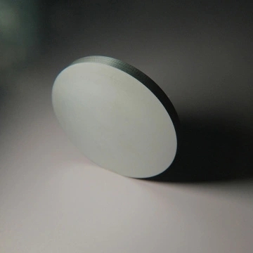
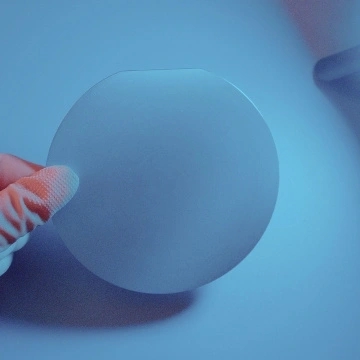
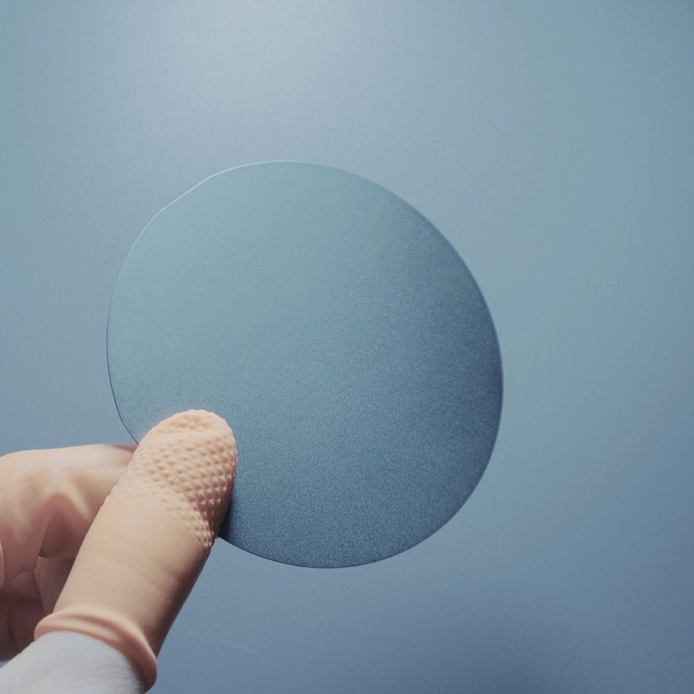
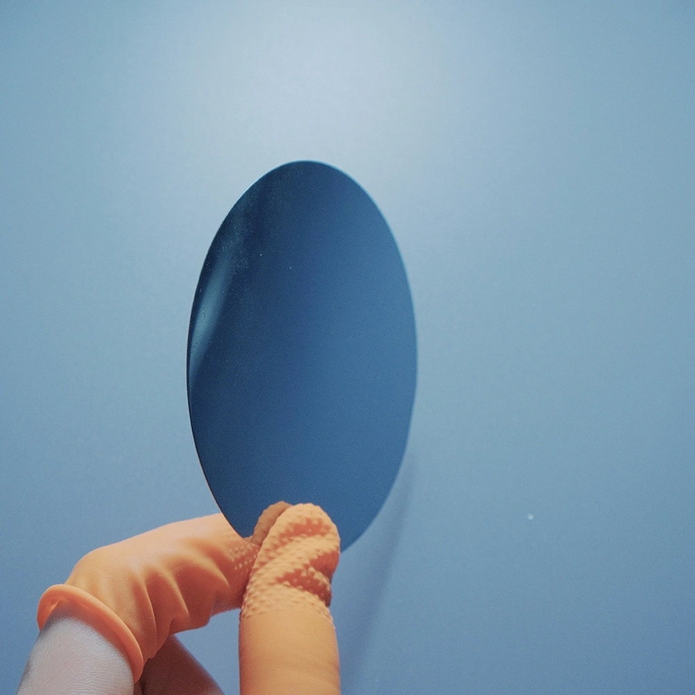
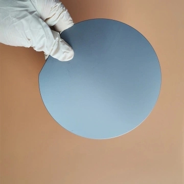
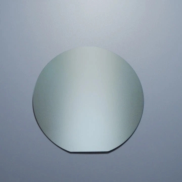
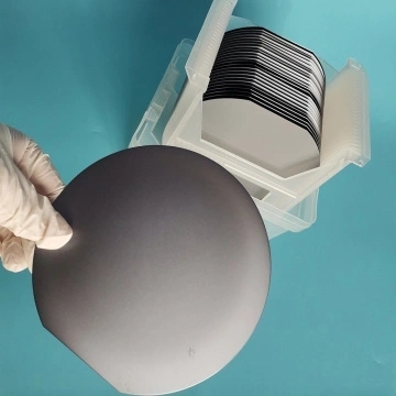
Zoolied provides SOI (Silicon on Insulator). SOI wafers use silicon-insulator-silicon substrates for specific applications where reducing parasitic capacitance of devices is critical. Many photonic devices also use SOI wafers to make thin silicon optical channels, integrated heaters, and other optical devices. They are also used in MEMS production, where thin Si layers are patterned and etched, and the underlying insulator layer is removed by selective etching to leave independent features. These applications include strain gauges, resonant cantilevers for AFM and molecular scale manipulators, and microfluidic devices.
The following are the parameters of the SOI chip.
1. Device thickness
This is the thickness of the top layer of silicon, usually in microns.
2. Growth method
This is listed twice in the SOI wafer. The first is the growth method of the device layer, which can be CZ or FZ.
3. Device resistivity
Measured with a standard silicon wafer, this is the resistivity of the top silicon layer in Ohm-cm.
4. Box
This is the thickness of the insulator or "buried oxide" layer, so it is BOx. As with all thicknesses, it is usually µm, but it can also be nm or Å.
5. Handle thickness
The thickness of the silicon bottom layer, usually in µm.
6. Growth method
The second list of growth methods involves the silicon processing layer.
7. Dealing with resistivity
Measured with a standard silicon wafer, this is the resistivity of the silicon bottom layer in Ohm-cm
8. Back
This is related to the processing method of the back side of the processing layer, which can be various finishes, including: polishing, etching, oxidation, non-oxidation and laser marking.
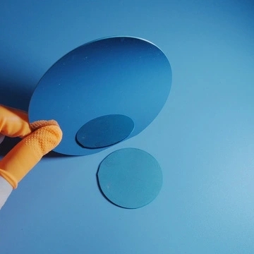
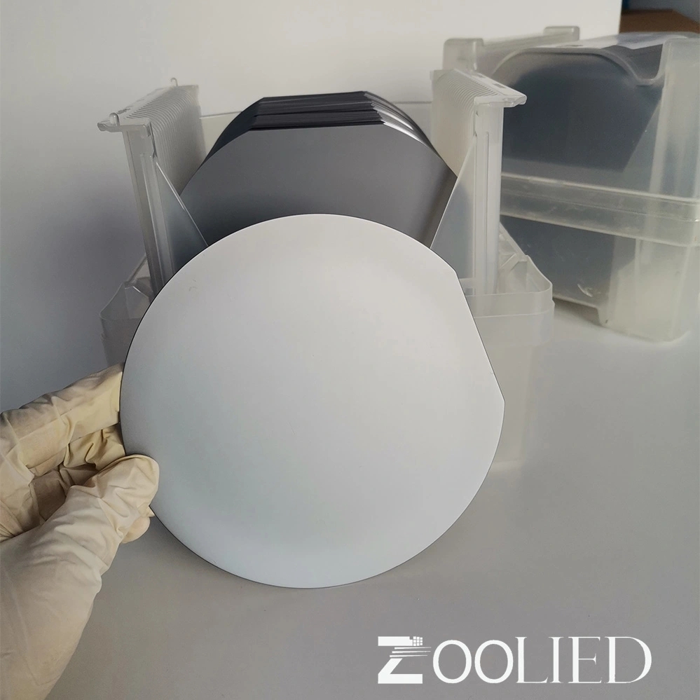
Zoolied offers a variety of optical Glass Wafers, such as Dummy Silicon Wafers, Jgs1 Wafers, and K9 Wafers, and Bk7 Wafers. ZOOLIED provides multiple anti-reflection coating options and also provides uncoated optical glass wafers. Looking for ideal optical si wafers and Ge Wafers Manufacturer & supplier? We have a wide selection at great prices to help you get creative. All the optical glass wafers are quality guaranteed. Zoolied is China Origin Factory of optical Wafers. If you have any question, please feel free to contact us.
Note: Please pay attention to your email at any time after inquiring, we will send you the quotation by email.
| Zoolied Standard Silicon Wafer | |||||||
| Diameter | 2" | 3" | 4" | 5" | 6" | 8" | 12" |
| Grade | Prime/ Test/ Dummy | ||||||
| Growth Method | CZ/FZ | ||||||
| Orientation | < 100 > , < 111 > , < 110 > | ||||||
| Type/Dopant | P/Boron , N /Phos, N /As, N /Sb | ||||||
| Thickness (um) | 279 | 380 | 525 | 625 | 675 | 725 | 775 |
| Thickness Tolerance | Standard ± 25μm | ||||||
| Resistivity | 0.001 - 10,000ohm-cm | ||||||
| Surface Finished | DSP,SSP | ||||||
| TTV (um) | Standard < 10 um | ||||||
| Bow/Warp (um) | Standard <40 um | ||||||
| Particle | Specified by customer | ||||||


-
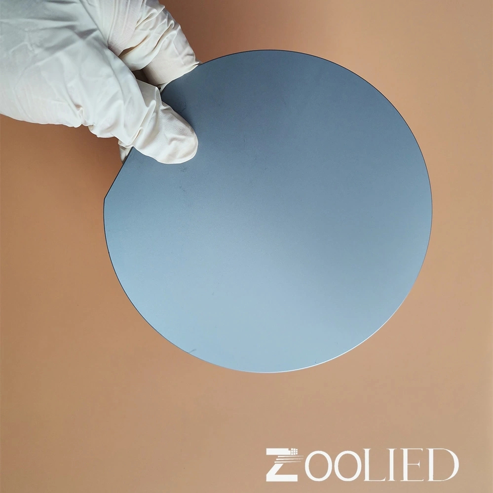
 50.8mm 76.2mm 100mm Silicon oxide wafer
-
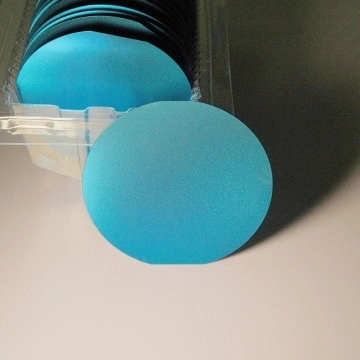
 SSP 100mm 500um P Silicon oxide wafer
-
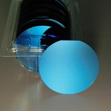
 DSP 100mm 360um 2-3Ω.cm N Silicon wafer
-
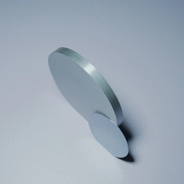
 SSP 100mm 500um Silicon wafer
-
 100mm 500um Silicon wafer
-
 SSP 100mm 500um 1-10Ω.cm N Silicon wafer
-
 SSP 50.8mm 420um >2000Ω.cm N Silicon wafer
-
 SSP 50.8mm 500um 5000-8000Ω.cm N Silicon wafer
