
Semiconductors are the core of electronic products, the cornerstone of the information industry, and are also known as the "food" of modern industry. But how much do we know about Silicon Wafers, the core material for making semiconductors? What is silicon wafers? Silicon wafer is the basic material for making semiconductor chips, it is the second most common element in the earth's crust, accounting for about 26%, second only to oxygen (49%). Silicon is widely present in high-concentration sand, gravel and rocks in the form of quartz (silica) in nature. Then through a series of complex processes such as purification and processing, it becomes the basic raw material-silicon wafer that meets the requirements of producing integrated circuits.
The production of silicon wafer usually has the following steps:
1) long crystal, which can be divided into CZ and FZ, because the fused polycrystalline material will directly contact with the quartz crucible, so the impurities in the quartz crucible will contaminate the fused polycrystalline. The CZ method is suitable for drawing large-diameter (300 mm) silicon wafers, which is the main Semiconductor Silicon Wafer material at present. As the polycrystalline raw materials are not in contact with the quartz crucible, there are few internal defects and low carbon and oxygen content, but the price is expensive and the cost is high. It is suitable for high-power devices and some high-end products.
2) slicing and drawing of the single crystal silicon rod need to cut off the head and tail material, then roll and grind it to the required diameter, cut the flat edge or V groove, and then cut into thin silicon wafer. At present, diamond wire cutting technology is usually used, with high efficiency and good warpage and curvature of silicon wafer. A small number of special shaped pieces can be cut with an inner circle.
3) grinding: after slicing, the damaged layer on the cutting surface needs to be removed by grinding to ensure the quality of the silicon wafer surface, about 50um.
4) corrosion: corrosion is to further remove the damaged layer caused by cutting and grinding, so as to prepare for the following polishing process. Corrosion usually includes alkali corrosion and acid corrosion. At present, due to environmental factors, most of them adopt alkali corrosion. The removal amount of corrosion can reach 30-40um, and the surface roughness can also reach micron level.
5) polishing: polishing is an important process for silicon wafer production. Polishing is to further improve the surface quality of silicon wafer through CMP (chemical mechanical polished) technology, so that it can meet the requirements of chip production. After polishing, the surface roughness is usually RA < 5A.
6) cleaning and packaging: as the linewidth of the integrated circuit is getting smaller and smaller, the requirements for improving the particle size index are getting higher and higher. Cleaning and packaging is also an important process for silicon wafer production. Most particles attached to the surface of silicon wafer > 0.3um can be cleaned by megasonic cleaning, and then the silicon wafer surface can be made by vacuum sealing packaging or inert gas packaging with a plug box free of cleaning The surface cleanliness meets the requirements of IC.
Characteristics of silicon wafer
Silicide has good electrical conductivity, high temperature resistance, resistance to electromigration and other characteristics. Silicon shrinks in volume when it is melted, and conversely, expands in volume when solidified from a liquid state. It can be used to prepare leads, resistors and other components inside integrated circuits. Silicon has no ductility at room temperature and is a brittle material. However, when the temperature is higher than 7000°C, silicon has thermoplasticity and will deform plastically under stress. The tensile stress of silicon is much greater than the shear stress, so the silicon chip is easily broken. Thin Si Wafers are sometimes bent during processing, which affects the accuracy of lithography.
Residual stress and surface processing damage in a silicon single crystal Glass Wafers have a great influence on its mechanical properties. The more serious the surface damage, the worse the mechanical properties. However, the silicon dioxide layer formed after heat treatment can play a role in healing the "wound" and increase the strength of the material.
Silicon is the main semiconductor material for making microelectronic devices and integrated circuits, but it has two shortcomings as an optoelectronic material: it is an indirect band gap material and cannot be used for lasers and light-emitting tubes; secondly, it has no linear electro-optical effect and cannot be used as modulators and switches.
Application of silicon wafer
The application of silicon chips covers almost all aspects of our lives and is the basis of electronic "chips". A wide range of new applications in the Internet of Things, wearable and mobile devices, self-driving cars, cloud computing, 5G communication networks, etc. actually ensure that the demand for thin prime and Dummy Silicon Wafers will continue to accelerate growth.
In addition, silicon is mainly used in diodes, solar cells, and integrated circuits, and can also be used as a substrate for epitaxial wafers. For example, memory circuits usually use Cz polished wafers, mainly because of their lower cost. The current diameter of CZ silicon wafers can be controlled between 3 and 12 inches. MCZ silicon and CZ silicon are basically similar in use, but their performance is better than CZ silicon.
FZ silicon is mainly used in the field of high-voltage and high-power controllable rectifier devices, and is commonly used in the chips of high-power transmission and transformation, electric locomotives, rectification, frequency conversion, mechatronics, energy-saving lamps, televisions and other products. The current FZ silicon wafer diameter can be controlled between 3 and 6 inches.
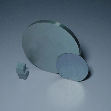
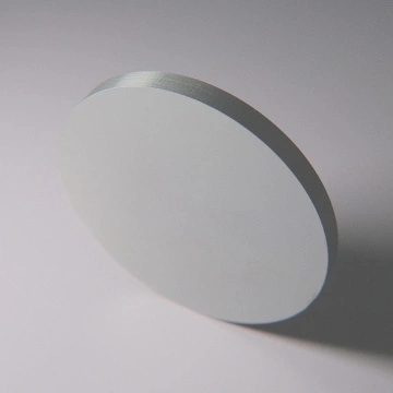
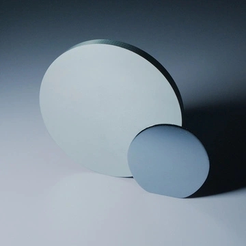
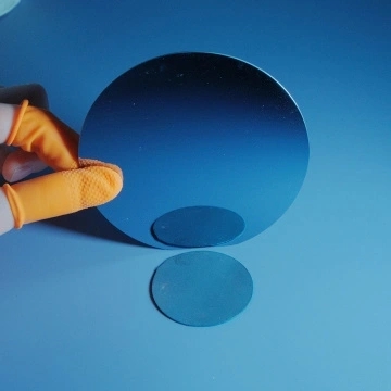
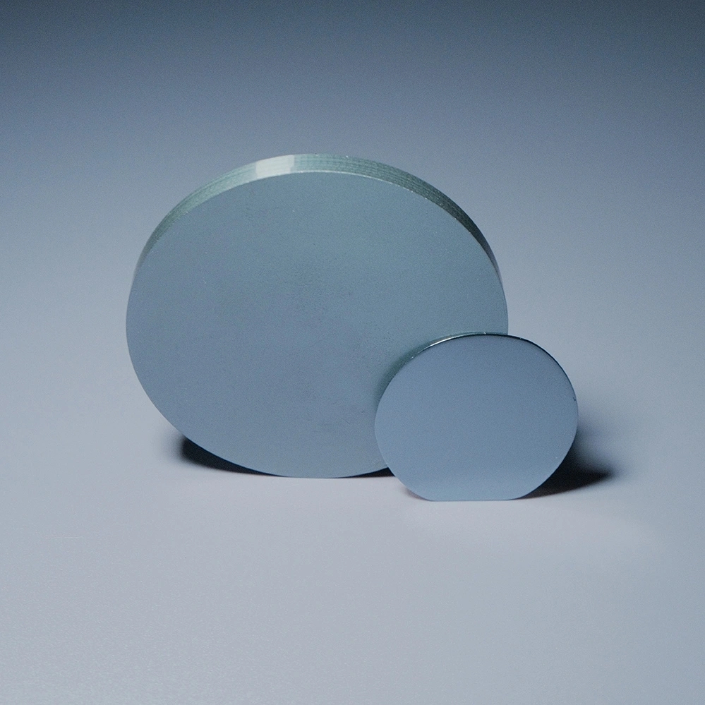
Zoolied offers a variety of optical glass wafers, such as dummy silicon wafers, Jgs1 Wafers, and K9 Wafers, and BK9 wafers. Zoolied provides multiple anti-reflection coating options and also provides uncoated optical glass wafers. Looking for ideal optical si wafers and Ge Wafers Manufacturer & supplier? We have a wide selection at great prices to help you get creative. All the optical glass wafers are quality guaranteed. Zoolied Inc. is China Origin Factory of optical Wafers. If you have any question, please feel free to contact us.
| Zoolied Standard Silicon Wafer | |||||||
| Diameter | 2" | 3" | 4" | 5" | 6" | 8" | 12" |
| Grade | Prime/ Test/ Dummy | ||||||
| Growth Method | CZ/FZ | ||||||
| Orientation | < 100 > , < 111 > , < 110 > | ||||||
| Type/Dopant | P/Boron , N /Phos, N /As, N /Sb | ||||||
| Thickness (um) | 279 | 380 | 525 | 625 | 675 | 725 | 775 |
| Thickness Tolerance | Standard ± 25μm | ||||||
| Resistivity | 0.001 - 10,000ohm-cm | ||||||
| Surface Finished | DSP,SSP | ||||||
| TTV (um) | Standard < 10 um | ||||||
| Bow/Warp (um) | Standard <40 um | ||||||
| Particle | Specified by customer | ||||||


